The final report as submitted for ENGR 113 on June 11, 2026, with contact emails removed.
ENGR 113 - Spring 2024First-Year Engineering Design
Ultra-high-speed optical fiber communications for massive parallel processing systems used in artificial intelligence
- Date Submitted: June 11, 2026
- Submitted to:
- Afshin Daryoush
- Group Members:
- Zach Busch
- Nicholas Gazzara
- Jonas Craig
Abstract
This freshman engineering design project developed an ultra‑high‑speed optical fiber communication system for massively parallel AI processing. With the AI market projected to reach $1.339 trillion by 2030, data centers must scale in bandwidth, efficiency, and cost, driving the need for improved communication architectures. The project aimed to maximize optical link performance while remaining cost‑effective. Key challenges included defining the system architecture, selecting photonic and computer hardware, and creating a clear, readable block diagram. Although NVIDIA hardware was initially considered, Infinera optical solutions were ultimately chosen for their scalability. Technical work included calculating signal‑to‑noise ratio (SNR), bit‑error rate (BER), bandwidth, and latency. Additional tasks involved environmental and cost analysis, literature review, and preparing presentation materials. Overall, the project provided practical experience in system‑level engineering and the challenges of designing next‑generation optical communication systems for AI.
Introduction
The rapid growth of artificial intelligence has created a significant increase in demand for high-performance computing systems. As AI models become larger and more complex, they require greater data movement, higher bandwidth, and continuous system operation. This places increasing pressure on modern data center infrastructure, particularly in terms of scalability, efficiency, and power consumption. The goal of this project is to examine these challenges and explore how large-scale computing systems can better support AI workloads.
Problem Overview
In the last few years, modern LLMs have exploded in popularity, creating a large demand for high-performance computing among consumers and industry alike. This growth has created demand not only to further develop AI models, but also to develop the computing hardware required to run them. As AI models have become significantly more advanced, they have also become increasingly complex. Today, AI training workloads can require thousands of flagship, high-power GPUs to develop and train effectively. [1] These GPUs are configured in servers to maximize bandwidth and create fast connections from GPU to GPU. These systems allow GPUs to constantly exchange model parameters, gradients, and training data. [2] Because of this data transfer requirement, the underlying system connecting GPUs has become nearly as important as the GPUs themselves. This GPU-to-GPU communication infrastructure has been heavily researched and invested in by companies such as Nvidia, Google, Microsoft, Meta, and many other cloud service providers.
This GPU-to-GPU communication link has become much more complicated in recent years. Today, communication occurs across multiple “layers” within an AI computing architecture. These layers range from communication within a rack, to rack-to-rack, pod-to-pod, and finally building-to-building communication. While technologies such as NVLink Gen 5 have heavily optimized communication within servers and racks, communication between pods and buildings still has significant room for improvement. [3] Currently, this communication is commonly handled using technologies such as Ethernet or InfiniBand. Large deployments using these technologies often rely on fat-tree and Clos network architectures. [4] These deployments are capable of providing high performance, but often at the cost of increased complexity and reduced scalability as systems continue to grow.
As a result, as AI systems grow, more data must be moved from rack to rack, pod to pod, and building to building. As physical link lengths increase, latency, BER, and power consumption can increase significantly. Traditional communication technologies such as Ethernet and InfiniBand face additional challenges, including signal integrity concerns and bandwidth limitations. [1] Additional network layers built upon these technologies can further increase system complexity while reducing overall scalability. As AI systems continue to expand, the demand placed on these communication links grows as well. [2] Consequently, many companies are searching for faster, more efficient, and more scalable methods of data communication.
One of the most promising solutions is optical fiber communication. Optical fiber has the ability to provide significantly higher bandwidth than traditional copper connections while maintaining very low attenuation over long distances. A technology known as Wavelength Division Multiplexing (WDM) allows multiple independent data channels to operate simultaneously on a single fiber. [5] Technologies such as WDM improve scalability while helping reduce overall power consumption. With the recent growth of AI computing, researchers have increasingly turned toward optical networking as a potential solution for future AI infrastructure. Because future AI systems will require scalable, high-bandwidth communication between racks, pods, and buildings, optical networking architectures have emerged as a promising solution to overcome the limitations of traditional electrical interconnects.
Existing Solutions and Marketability
As mentioned previously, many companies have invested significant amounts of time and resources into researching AI communication architectures. For example, Nvidia has developed AI systems utilizing technologies such as NVLink and NVSwitch to provide high-bandwidth communication within servers and racks. [4] Nvidia also commonly utilizes InfiniBand in large-scale deployments built around fat-tree (Clos) architectures. [4] Google has approached this challenge through TPU Pods, which use torus-based interconnects designed to efficiently support distributed AI training workloads. [2] Microsoft has addressed similar challenges using Ethernet leaf-spine architectures, providing scalable communication across large data center deployments. [6z] Each of these approaches successfully supports modern AI workloads; however, as AI systems continue to increase in size and complexity, these solutions become increasingly expensive and difficult to scale.
Today, AI infrastructure spending continues to grow rapidly. As AI models become more capable, data centers require communication solutions that provide greater bandwidth while minimizing latency. Additionally, power consumption has become a major design consideration. Optical networking technologies are already widely used throughout telecommunications and internet backbone infrastructure. Emerging technologies such as WDM, coherent optics, and photonic integrated circuits are being actively researched and developed for future AI networking applications. [5], [7], [8], [9] A scalable AI architecture utilizing these technologies could significantly reduce communication bottlenecks while improving efficiency and long-term scalability. These industry trends indicate a growing demand for scalable optical communication systems capable of supporting next-generation AI workloads, motivating the development of the architecture proposed in this project.
Project Objectives and Deliverables
The objective of this project was to develop a scalable communication architecture for large AI computing systems. The proposed design uses four layers to form a complete AI server communication architecture. Layer 1 utilizes Nvidia’s GB300 compute trays, serving as the primary compute layer of the system. Layer 2 utilizes Nvidia’s NVL72 rack architecture, providing high-bandwidth copper connections between compute trays. Layer 3 employs a Polatis Series 7000 optical circuit switch to provide high-bandwidth rack-to-rack connectivity. [10], [11] Layer 4 uses the Infinera 1830 GX G42 and FlexILS DWDM transport system to provide pod-to-pod and long-distance communication. [7] This architecture emphasizes scalability, bandwidth efficiency, and communication reliability to support future AI computing systems.
The project’s deliverable was to design a scalable and efficient AI server communication architecture utilizing optical fiber technologies. The proposed solution combines pre-existing commercial products and established networking concepts into a unified, scalable model. The primary goal is to improve data movement across multiple layers of the system, ranging from rack-to-rack communication to pod-to-pod communication. To evaluate the design, the group considered performance metrics such as bandwidth, latency, SNR, and BER. Additional engineering considerations included cost, reliability, scalability, and implementation complexity. The final deliverable was a complete architectural design supported by system diagrams, engineering calculations, and technical justification.
Technical Activities
In the beginning of the project, the group conducted research on modern AI data center architectures and communication methods. This research focused on technologies such as Nvidia NVLink, InfiniBand, Ethernet leaf-spine networks, and Google TPU pod interconnects. Following this, the group reviewed optical networking technologies including WDM, DWDM, PAM4 modulation, and coherent optical communication. Through this research, several limitations of existing AI communication systems were identified, including scalability constraints, increasing latency, bandwidth bottlenecks, and communication reliability challenges. This research provided a sturdy foundation for the remainder of the project and helped guide future design decisions.
Following this, the group spent the remaining time optimizing and refining the selected system. The group narrowed the architecture down to four layers and began analyzing the best base computing layer. After additional research, the group settled on the GB300 compute board and NVL72 rack architecture. The group added the Polatis optical circuit switch and Infinera DWDM transport system to unify the building’s architecture. Finally, the group analyzed how each layer communicates with one another and how data flows throughout the system. The project’s goal was to place an emphasis on optical fiber technology, so the final architecture utilized it where it fit best. This helped strengthen the scalability of the system while also reducing power usage. Several architecture revisions were made throughout the design process before the final hierarchy was selected.
The last step of the project was to perform an engineering analysis and finalize the architecture. First, the group performed technical calculations covering bandwidth, SNR, and BER. The group used these calculations to compare distinctive design choices and identify the strongest options. Next, the group analyzed wavelength allocation, DWDM channel spacing, and different optical transmission characteristics. Additional research was conducted to verify that the selected optical technologies would support future scalability requirements. Finally, the group performed a final evaluation of the architecture’s scalability and examined the system operating across multiple buildings. The group also performed environmental impact calculations, including power consumption and cooling requirements. Lastly, the group converted this information into a final system diagram (Fig. 1), a presentation, and a final paper outlining the completed design.
Weekly Progress
Week 1: The project was introduced, and initial requirements were reviewed. Background research began on artificial intelligence systems and data center infrastructure.
Week 2: Research continued on data center architectures and communication methods. Networking technologies such as InfiniBand and Ethernet were also explored.
Week 3: Work focused on high-speed interconnects and early exposure to optical communication concepts. Key challenges such as scalability and bandwidth limitations were identified.
Week 4: Optical networking topics such as wavelength division multiplexing and optical switching were studied in more detail.
Week 5: Time was spent continuing optical networking research while starting to think about possible system structure and organization.
Week 6: System architecture ideas were developed and refined. Real world components and technologies used in AI infrastructure were also reviewed.
Week 7: Focus shifted toward environmental impact, including power consumption, heat generation, and cooling requirements.
Week 8: Cost considerations and system scaling were explored. Work also began organizing content for the presentation.
Week 9: Presentation slides and visuals were developed. Preparation for final presentation also began.
Week 10: The final presentation was completed, reviewed, and prepared for submission.
Project Timeline
TABLE I FRESHMAN DESIGN PROJECT TIMELINE
| Task | Week 1 | Week 2 | Week 3 | Week 4 | Week 5 | Week 6 | Week 7 | Week 8 | Week 9 | Week 10 |
|---|---|---|---|---|---|---|---|---|---|---|
| Literature Review / Background Research | X | X | X | X | ||||||
| Learning Optical Networking Concepts | X | X | X | X | ||||||
| System Architecture Design | X | X | X | |||||||
| Component Selection | X | X | X | X | ||||||
| System Scaling & Configuration | X | X | X | X | X | |||||
| Environmental & Sustainability Analysis | X | X | X | X | X | |||||
| Cost Analysis & Power Modeling | X | X | X | X | X | |||||
| Slide Development & Visualization | X | X | X | |||||||
| Presentation Preparation | X | X | X | |||||||
| Final Report Writing & Revisions | X | X |
Project Budget (how much did it cost to create the prototype) - Nicholas
Table 2: Estimated Project Budget for GB300-Based AI Data Center System
| Component / System Level | Description | Estimated Cost |
|---|---|---|
| GB300-Class Compute Node | Grace CPU + Blackwell GPU + NVLink architecture | ~$30,000 - $50,000 per node |
| Rack (18 trays) | GB300 compute + NVLink fabric (single compute domain) | ~$2.7M - $3.6M |
| Pod (8 racks) | Scaled compute cluster + intra-pod networking | ~$22M - $29M |
| Full System (64 racks total) | 1,152 trays + optical fabric (OCS) + InfiniBand cluster networking | ~$180M - $230M |
Results
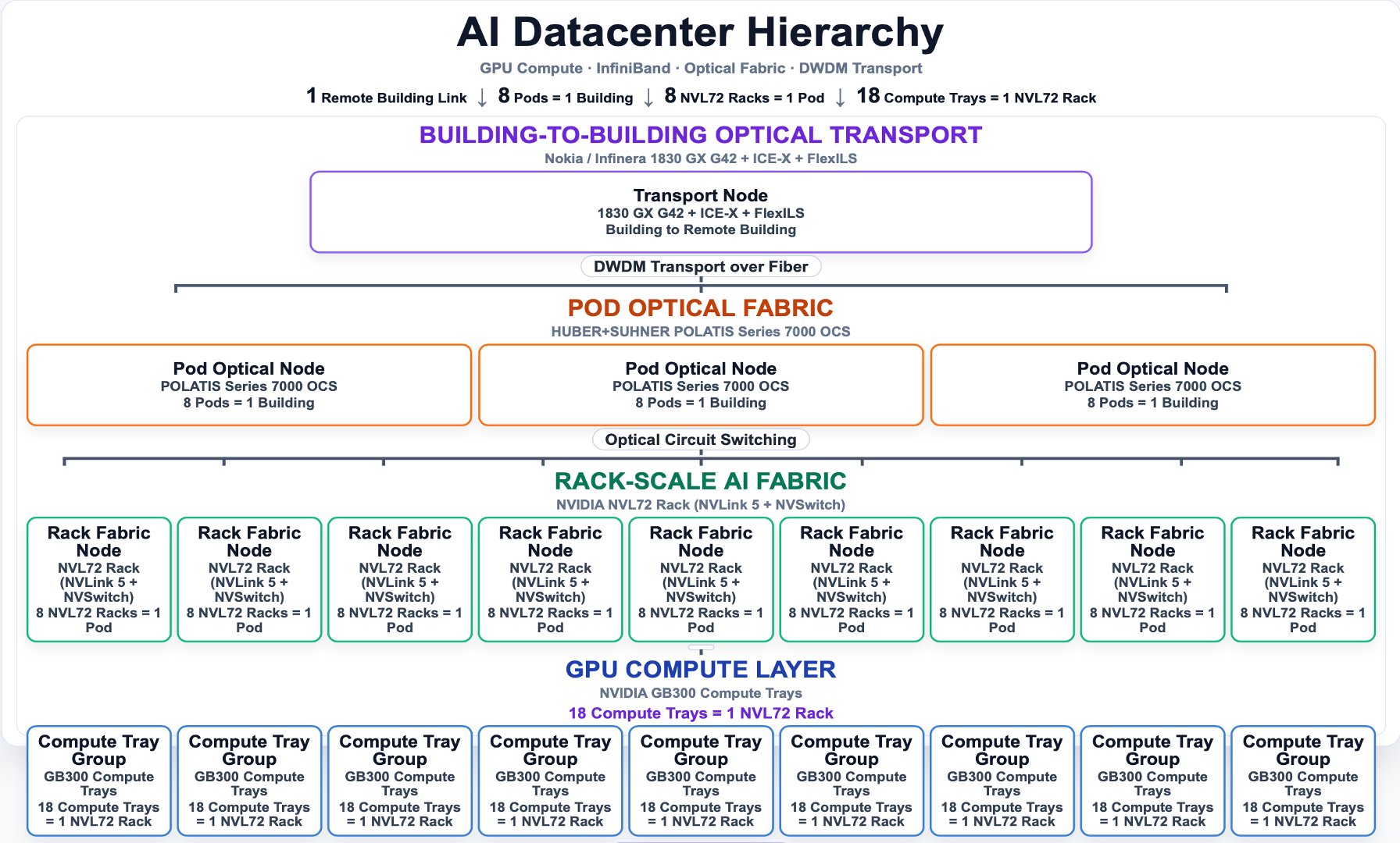
Fig 1. Proposed AI datacenter communication hierarchy consisting of NVIDIA GB300 compute trays, NVL72 rack-scale fabrics, Polatis optical circuit switches, and Infinera DWDM transport systems.
After months of research and development, the group landed on a final system architecture. The final communication hierarchy developed during this project is shown in Fig. 1. It consists of four layers. Layer one, being the compute layer, is made up of Nvidia’s GB300 compute trays [15]. Following this, Layer 2 uses Nvidia’s NVL72 rack architecture [1]. Layer one and two are preconfigured and deeply optimized already by Nvidia. Layer 3 and 4 are where the group's research was primarily focused. Layer 3 utilizes the Polatis Series 7000 SMT Optical Circuit Switch [10], [11]. This is what redirects traffic from rack to rack in each pod. Finally, Layer 4 uses an Infinera 1830 GX G42 and FlexILS DWDM Transport system to move data between each pod within a data center [7].
This data starts processing at Layer 1, the GB300 compute tray. These boards are made up of 4 B300 Blackwell GPUs wired to 2 ARM-based Grace CPUs [15]. These chips communicate with Nvidia’s proprietary NVLink C2C system, providing an ultra-high-bandwidth, low-latency chip-to-chip connection [15]. These compute racks are vital to the entire architecture. The remaining architecture is designed to connect these boards to each other on a massive scale. Because of this scale, bottlenecks are inherently from Layers 2 to 4, which are designed to reduce these as much as possible.
Continuing onto Layer 2, each compute tray is connected to the NVL72 rack spine. This spine uses the NVLink Gen 5 protocol from Nvidia to again maximize bandwidth and minimize latency [3]. These racks exist to cluster together different “nodes” of GB300 boards. This system is already designed and optimized by Nvidia. Nvidia describes one NVL72 rack as “essentially one giant GPU” [1]. Data is outputted from the NVL72 rack in PAM4 modulation over single-mode fiber running at 1310 nm [12], [13].
At Layer 3, the group selected the Polatis Series 7000 SMT Optical Circuit Switch. This selection was made specifically to maximize bandwidth [10], [11]. Specifically, within our architecture, the Polatis Series 7000 SMT OCS receives all the aggregated traffic from the NVL72 racks and begins preparing this data for long-distance transport. Because the switch is entirely optical, SNR is kept as high as possible, reducing BER [14]. In addition to preserving signal quality, the optical circuit switch provides a non-blocking switching architecture, allowing multiple optical paths to exist simultaneously without creating network congestion [10], [11], [14]. This capability is primarily why the group chose this specific model switch for Layer 3. Layer 3 outputs the same single-fiber PAM4 encoded signal at 1310 nm that was inputted [12].
Finally, Layer 4 is the final networking layer of this architecture. At this stage, the objective switches from low-latency switching to long-distance data transmission. At this stage, the encoded PAM4 data is inputted into the Infinera GX G42 transport platform [7]. The group utilized Infinera’s ICE-X coherent optical technology to convert the incoming PAM4 signal into multiple data streams formatted into DWDM channels for long-distance transmission [5], [7], [9]. By leveraging these technologies, the group is able to continue to optimize SNR and BER while still maintaining a high-bandwidth signal at low latency [7], [9].

Fig 2. Calculations for the SNR, BER, and Bandwidth in layers 1-4 of the system.
The group took this architecture and analyzed it further with calculations. The group reviewed BER, SNR, and bandwidth. The bandwidth between Layers 1 and 3 was analyzed to determine the amount of data that can be transferred throughout the architecture. The resulting bandwidth was found to be 112 Gbps for layer 1, and 800 Gbps for layers 2 and 3 (Fig 2.). The total building bandwidth was calculated based on the overall system configuration and communication architecture. The resulting bandwidth was determined to be 800 Gbps overall (Fig 2.). The signal-to-noise ratio (SNR) of the optical communication system was calculated and found to be 55 dB (Fig 2.). These calculations help validate the feasibility of the proposed architecture and support its use in future AI computing systems. Using the calculated SNR value, the bit error rate (BER) was determined to be 10^-17 (Fig 2.).
Overall, the goal of the group was to create an architecture using pre-existing technologies all combined into one unified system designed to utilize optical fiber for scalability and efficiency. The group utilized Nvidia’s technologies in conjunction with Polatis and Infinera to maintain high bandwidth at long-distance scales. This is directly where the use of optical fiber fits into the architecture, as it provides significantly higher bandwidth and lower attenuation than traditional copper-based communication links. By integrating these technologies, the proposed system is able to reduce communication bottlenecks between racks, pods, and buildings while maintaining low latency and reliable data transmission. As AI systems continue to grow in size and complexity, architectures such as this may provide a scalable framework capable of supporting future computing demands.
Discussion
The prototype did well in terms of meeting the requirements for the given original problem of solving the issue with massive parallel optical network systems for Artificial intelligence. The values given for the different layers were all within standard. Such a system would be marketable to only a very specific company or application. Such a system would cost around 180-200 million dollars. This is not something for the average small consumer or data server company. Only large-scale corporations can afford this kind of network. Possibly this could be scaled down by condensing the layers and having less hardware, but there would be a significant loss in performance for the end user. With the increase in artificial intelligence, marketing will almost sell itself. If one could offer this as a package deal to the end user, that would be ideal. There would be less of a headache for doing specific calculations for any type of data transfer on their end, and being able to leave space for upgradability is also beneficial, with the speed of artificial intelligence hardware development. Possibly selling smaller or larger scale versions of this could bring in a larger and more accessible customer base. Even customers who are new to the space of artificial intelligence. To bring this product to market, a full-size version of this needs to be tested in real life, with all the servers. The initial investment of this will be costly, but in the long term it will be worth it. First, having a fully functional test bed, one can see how much electricity is being pulled by the system when artificial intelligence is running, as well as any contribution of heating if there is any. This will also serve as a great demonstrator of potential buyers of the system, for this will answer any questions there are. Once the actual system has been made at least once, then it can be put into any environment or application that is desired. So, the marketing of the product is quite simple, since the actual system is constructed, and clients can tour it. Although the cost of capital is incredibly high, in the long run it will be worth it. The system needs further testing, especially as a fully integrated system with other models, such as Claude and OpenAI, as running it in different environments can present different data rates and power usage. Also, one needs to test how this system will work with different LLM’s, such as those for research or other types of highly advanced computing systems.
Impact Statement
The GB300-based AI data center architecture we designed has both sustainability benefits and broader societal impacts. By using optical networking technologies like Optical Circuit Switching (OCS) and Dense Wavelength Division Multiplexing (DWDM), the system can transmit large amounts of data more efficiently, reducing the need for additional physical infrastructure and lowering network power consumption [16]. However, the overall system still operates at a very large scale, with 64 racks and 1,152 compute trays connected through NVLink and InfiniBand, which results in a multi-megawatt continuous power demand and significant heat generation [17]. This requires advanced cooling systems and increases both energy and water usage, making efficiency a critical factor in system design. As data centers continue to expand to support AI workloads, their impact on electricity consumption and carbon emissions becomes more significant, highlighting the need for more sustainable operation and energy-aware computing strategies [18]. The critical nature of this need is understood by federal projections indicating that national data center electricity consumption could near 6,000 gigawatt-hours by 2028, capturing between 6.7% and 12% of the total U.S. energy grid (see Fig. 3) [19]. While systems like this enable major advancements in areas such as research, healthcare, and automation, they also emphasize the importance of balancing high-performance computing with responsible energy use and long-term environmental sustainability.
Chart not reproduced here (third-party graphic).
Fig. 3. Historical and projected total U.S. data center electricity consumption from 2014 to 2028, showing a range of future national power demand [19].
References
[1] “NVIDIA’s AI Factory Drives Enterprise Innovation at Scale,” NVIDIA AI Factory, 2026. https://www.nvidia.com/en-us/case-studies/ai-factory-drives-enterprise-innovation-at-scale/
[2] N. P. Jouppi et al., “In-Datacenter Performance Analysis of a Tensor Processing Unit,” Proceedings of the 44th Annual International Symposium on Computer Architecture - ISCA ’17, 2017, doi: https://doi.org/10.1145/3079856.3080246.
[3] D. Foley and J. Danskin, “Ultra-Performance Pascal GPU and NVLink Interconnect,” IEEE Micro, vol. 37, no. 2, pp. 7-17, Mar. 2017, doi: https://doi.org/10.1109/mm.2017.37.
[4] C. Gomez, F. Gilabert, M. E. Gomez, P. Lopez, and J. Duato, “Beyond Fat--tree: Unidirectional Load--Balanced Multistage Interconnection Network,” IEEE Computer Architecture Letters, vol. 7, no. 2, pp. 49-52, Jul. 2008, doi: https://doi.org/10.1109/l-ca.2008.8.
[5] “Optical WDM Networks: Concepts and Design Principles | IEEE eBooks | IEEE Xplore,” Ieee.org, 2026. https://ieeexplore.ieee.org/servlet/opac?bknumber=5263048 (accessed Jun. 12, 2026).
[6] M. Tavares, R. Valadas, T. Amado, M. Paz, and S. Santos, “Decentralized and Dynamic Zero-Touch Provisioning of Leaf-Spine EVPN Data Centers,” IEEE Access, vol. 13, pp. 125190-125206, 2025, doi: https://doi.org/10.1109/access.2025.3589509.
[7] Z. Fan, Y. Dan, T. Zhang, J. Dai, and K. Xu, “Tandem Neural Network Based Rapid Voltage Configuring Method for Programmable Photonic Integrated Circuit,” 2024 Asia Communications and Photonics Conference (ACP) and International Conference on Information Photonics and Optical Communications (IPOC), pp. 1-3, Nov. 2024, doi: https://doi.org/10.1109/acp/ipoc63121.2024.10809891.
[8] E.-H. Lee, “Optical Printed Circuit Board (O-PCB) as a Platform for VLSI Micro/Nano-Photonic Circuits and Networks,” Jul. 2007, doi: https://doi.org/10.1109/icton.2007.4296074.
[9] H. Zhang, Z. Jia, L. A. Campos, and C. Knittle, “Experimental Demonstration of Rate-Flexible Coherent PON Up to 300 Gb/s,” Journal of Lightwave Technology, vol. 42, no. 16, pp. 5440-5449, Aug. 2024, doi: https://doi.org/10.1109/jlt.2024.3366163.
[10] Venkata Virajit Garbhapu, G. Charlet, and Yvan Pointurier, “Optical Networks for Distributed AI Training: Flow Completion Time and Training Time Analysis,” pp. 1-6, May 2025, doi: https://doi.org/10.23919/ondm65745.2025.11029332.
[11] “Optical Interconnects for large scale computing: How Do We Get Beyond the Cost & Power Wall?,” Ieee.org, 2021. https://ieeexplore.ieee.org/document/9489905 (accessed Jun. 12, 2026).
[12] “Experimental Demonstration of C-Band 112-Gb/s PAM4 over 20-km SSMF with Joint Pre- and Post-Equalization,” Ieee.org, 2020. https://ieeexplore.ieee.org/document/9083056 (accessed Jun. 12, 2026).
[13] Keysight, “PAM4 Design Challenges and the Implications on Test,” Keysight United States, 2026. https://www.keysight.com/us/en/assets/7018-04746/application-notes/5992-0527.pdf? (accessed Jun. 12, 2026).
[14] K. Ikeda, R. Konoike, and K. Suzuki, “Large-Scale and Multiband Silicon Photonics Wavelength Cross-Connect Switch With FSR-Free Grating-Assisted Contra-Directional Couplers,” Journal of Lightwave Technology, vol. 42, no. 12, pp. 4310-4316, Jun. 2024, doi: https://doi.org/10.1109/jlt.2024.3366553.
[15] “NVIDIA Blackwell Ultra Datasheet,” NVIDIA, 2025. https://resources.nvidia.com/en-us-blackwell-architecture/blackwell-ultra-datasheet?ncid=pa-srch-goog-251433 (accessed Jun. 12, 2026).
[16] K.-L. Lee, B. Sedighi, R. S. Tucker, H. (Keith) Chow, and P. Vetter, “Energy Efficiency of Optical Transceivers in Fiber Access Networks [Invited],” Journal of Optical Communications and Networking, vol. 4, no. 9, p. A59, Aug. 2012, doi: https://doi.org/10.1364/jocn.4.000a59.
[17] M. Dayarathna, Y. Wen, and R. Fan, “Data Center Energy Consumption Modeling: A Survey,” IEEE Communications Surveys & Tutorials, vol. 18, no. 1, pp. 732-794, 2016, doi: https://doi.org/10.1109/comst.2015.2481183.
[18] A. Radovanovic et al., “Carbon-Aware Computing for Datacenters,” IEEE Transactions on Power Systems, pp. 1-1, 2022, doi: https://doi.org/10.1109/tpwrs.2022.3173250.
[19] A. Shehabi et al., "2024 United States Data Center Energy Usage Report," Lawrence Berkeley National Laboratory, Berkeley, CA, USA, Rep. LBNL-2001637, Dec. 2024. [Online]. Available: https://eta-publications.lbl.gov/sites/default/files/2024-12/lbnl-2024-united-states-data-center-energy-usage-report_1.pdf